
Superresolution Cameras Empower Line-Scan Imaging
31 October 2026
Integrating software algorithms with both single-row and time delay integration arrays produces two images with half-pixel offsets that enable high-speed automatic optical inspection.
BY XING-FEI HE AND DALE DEERING, TELEDYNE DIGITAL IMAGING, AND DESHAN DUAN, BEIJING DAHENG IMAGING TECHNOLOGY
Machine vision requires increasingly higher performance and better detectability, but also lower system-level costs, for successful deployment in industrial environments. Line-scan
imaging has the capability to meet the requirements of today’s vision systems that integrate various technologies such as multispectral and multifield highspeed imaging1-4. However, hardware based solutions alone are not sufficiently adaptable to meet these rapidly changing requirements.
Superresolution technology
Superresolution (SR) emerged in the 1980s as a technique for multiframe signal reconstruction and found early practical application in airborne imaging, where platform motion naturally provides subpixel diversity. During the 1990s, spatial domain methods enabled operational resolution enhancement in airborne imaging systems, improving performance without requing more expensive optics. Although detector advancements have reduced dependence on SR, its system-level value has ensured its continued use in inspection applications, with many of today’s approaches still rooted in those early foundations.
SR technology, including versions patented by Teledyne Digital Imaging, leverages dual linear sensor arrays po sitioned with precise half-pixel offsets to achieve image quality beyond the native sensor capabilities (Figure 1)5. This approach doubles the effective pixel density, transforming input images into higher-resolution output images using unique algorithms. The technology supports both single-row and timedelay integration (TDI) arrays, enabling deployment across a wide range of line-scan applications, from mid-market web inspection to high-end precision semiconductor metrology, for detecting pinhole and particle defects.
And superresolution doesn’t just mean a target is “scaled up” digitally. Systems using this approach actually take multiple images of an object and use the extra data to create a higher definition output image.
SR imaging in a machine vision context consists of three primary stages: capture, reconstruction, and output. During image capture, dual sensor arrays simultaneously acquire offset images at native resolution. During the reconstruction stage, algorithms integrate the offset images, interleaving pixel data to generate the SR output. Data reconstruction can be executed in a host driver using control software, providing flexibility for systems with available CPU resources, or on a frame grabber for high-throughput processing.
From line scan to TDI
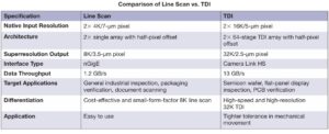
Two primary camera model types use SR technology, each with distinct performance profiles optimized for different applications. The first iteration delivers 8K SR output through dual
4K/7-μm arrays, utilizing a standard 2.5/10 Gigabit Ethernet interface for cost-sensitive applications with a maximum line rate of 75/82 kHz. This camera model performs well for general industrial inspection, packaging verification, and document scanning, where 8K resolution is sufficient.
For demanding subpixel and metrology applications, another camera achieves 32K/2.5-μm output resolution from dual 16K/5-μm TDI arrays, employing a Camera Link HS interface to support the substantial 13 GB/s data throughput with maximum 400-kHz line rates. This camera effectively targets semiconductor wafer, flat-panel display, and PCB inspection applications that require maximum spatial resolution (see Table below).
Both models feature the core dual array architecture with half-pixel offsets but differ in resolution, interface band width, and target application cases.
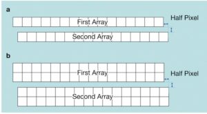
Figure 1.
Superresolution sensor architecture using two linear arrays with half-pixel offsets horizontally and vertically. The sensor array can be either a single-row array (a) or a multistage time delay integration (TDI) array (b). Images from both arrays are read out independently.
An SR line-scan system is easy to use since the gap between the two arrays is only ~10 μm. For TDI systems, however, the gap between the two TDI arrays is larger, at hundreds of micrometers. The larger gap requires tighter tolerances in mechanical movement design to ensure alignment between the camera and sample.
Differences exist between area camera SR and line-scan SR. With area-scan systems, the sensor is often shifted by microscale distances, which may affect the modulation transfer function (MTF) of the image due to blurring that can result from the movement. Line-scan and TDI systems do not move the sensor dynamically. It is possible to use up to four images to create a complete superresolution image, but generally, just two suffice if the image is shifted both horizontally and vertically.
Resolution, SNR, and MTF
As shown in Figure 2, SR technology delivers measurable improvements in both spatial resolution and signal to-noise ratio (SNR) compared with the native sensor resolution. Direct comparison of 16K/5-μm input versus 32K/2.5-μm superresolution output demonstrates visibly enhanced edge definition, finer feature reproduction, and reduced noise characteristics. The doubled pixel density enables detection of features at half the original pixel pitch, significantly improving the system’s spatial resolving power.
Beyond pure resolution gains, the dual-array averaging inherent in data reconstruction provides a significant improvement in signal-to-noise ratio, depending on defect characteristics
such as contrast. This SNR enhancement is particularly valuable for subpixel defect detection, where subtle gray level variations must be distinguished from sensor noise.
Existing applications in semiconductor inspection, flat-panel display verification, and precision PCB examination benefit substantially from the combined resolution and SNR improvements, enabling detection of defects previously masked by noise or below the native pixel size.
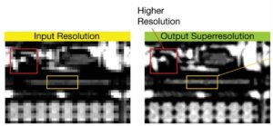
Figure 2.
A comparison of the original input 16K/5-μm image and the output 32K/2.5-μm superresolution image. The superresolution image provides higher resolution and a better signal-to noise (SNR) ratio.
The MTF quantifies an imaging system’s ability to reproduce contrastat varying spatial frequencies, serving as the definitive metric for optical resolution performance. SR technology demonstrates substantial MTF improvements across the spatial frequency spectrum compared with native sensor resolution (Figure 3). This MTF advantage translates directly to improved edge acuity, enhanced fine feature definition, and more reliable detectability. For line-scan flat-panel display inspection applications requiring 1- to 5-μm feature resolution at high line rates, the MTF improvement enables systems to operate at higher speeds while maintaining detection confidence.
A 32K/2.5-μm SR image significantly improves MTF compared with the input images from 16K/5-μm sensors. However, when compared with the image captured using a true 32K/2.5-μm pixel size, the SR resolution image has an inferior MTF (assuming a suitable lens has been selected for both cases). A simulation study carried out by the authors and colleagues indicated that SR technology provides an effective pixel size of ~3.5 μm with equivalent MTF performance (Figure 4). In other words, the output image’s MTF performance falls between that of an image with the native pixel size and that of an image with the output pixel size.
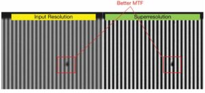
Figure 3.
Superresolution significantly improves the modulation transfer function (MTF). This is particularly important not only for defect detection but also for metrology, where contrast is paramount.
Subpixel defect detection
One of the challenges of optical inspection is subpixel defect detection. SR technology excels at detecting defects smaller than the native pixel pitch through combined resolution enhancement and noise reduction. Traditional single-array sensors struggle with subpixel defects (such as a subpixel pinhole) because the faint defect signal may be distributed across several pixels and easily obscured by sensor read noise. The dual-array architecture with half-pixel offsets enables defect energy to be sampled at intermediate positions, effectively qua
drupling the spatial sampling density. Simultaneously, the reconstruction algorithm’s inherent averaging reduces random noise, improving the SNR by a factor of four to five, depending on defect type and contrast characteristics.
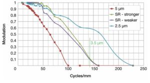
Figure 4.
The effective MTF of a superresolution camera falls between that of a camera with the native pixel size and that of a camera with the output pixel size. SR: superresolution.
In Figure 5, four regions of interest demonstrate this effect: ROI 1, ROI 2, and ROI 3 show subtle defects clearly resolved in the superresolution output but barely visible above the noise floor in conventional imaging, while ROI 4 represents the baseline noise floor for comparison. This performance advantage makes superresolution particularly valuable for semiconductor wafer inspection, flat-panel display defect detection, and PCB trace verification, where defects ranging from 1 to 5 μm must be reliably identified at production line speeds.
There are several ways to use the subpixel information, specifically through algorithms designed to combine the data into a composite image. For example, the algorithms can be used to reduce noise or for edge enhancement. Each of these approaches may be more or less beneficial to the end application, and the end user can select the exact parameters.
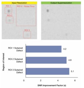
Figure 5.
Superresolution technology offers the best performance for detecting subpixel defects due to an improved SNR. Depending on the type of defect, the SNR can be improved by a factor of
four to five using superresolution. ROI: region of interest.
Benefits of superresolution
SR technology offers many benefits for real-world applications. First, it overcomes technical challenges in designing a small physical pixel in a CMOS sensor. A small pixel often comes with disadvantages, including low responsivity, small full-well capacity, and worse MTF than larger pixels. In particular, for TDI devices, a pixel smaller than 2.5 μm is technically challenging.
Second, a sensor with a small pixel requires an expensive optical lens. The high cost of the lens becomes prohibitive for many cost-sensitive applications in machine vision, such as PCB inspection.
Third, a sensor with a small pixel size also requires high-brightness lighting, which can generate significant heat and result in high maintenance costs. In addition, the degradation of high brightness LEDs over time also requires regular, costly replacement and maintenance.
Finally, SR technology reduces the data transmission and width requirement for a cable. After the pixel data is transferred from the camera through the cable, it doubles in the host or the frame grabber, reducing the amount of data going through the camera interface and the cable. The data reduction is significant because, in many applications, the data interface is the bottleneck in today’s high-performance vision systems.
Software meets hardware
Unlike conventional image upscalers, which use only software to expand a lower-resolution image, the physical pixel offsets used in SR technology capture real physical information in the pixel data. This feature preserves true image quality for machine vision applications.
Tuning the SR algorithm to achieve the best results requires knowledge of the application requirements and algorithm design. Furthermore, because camera resources are required to run these algorithms, highly efficient code and memory management are necessary to achieve the best results in real time. The capabilities of the CPU and PC memory are important considerations.
The previously described SR technology uses a software-defined pixel size based on a unique hardware pixel-offset sensor architecture, rather than software implementation alone. Solutions based on hardware combined with software innovation represent the future direction for meeting the demanding and rapidly changing image quality requirements of machine vision.
Meet the authors
Xing-Fei He is senior product manager at Teledyne Digital Imaging Inc. in Waterloo, Ontario, Canada; email: xing-fei. [email protected]. Dale Deering is vice president at Teledyne Digital Imaging Inc. in Waterloo, Ontario, Canada; email: dale. [email protected]. Deshan Duan is CEO at Beijing Daheng Imaging Technology Inc. in Beijing; email: [email protected].
References
1. X. He et al. (2012). Time delay integration speeds up imaging. Photonics Spectra, Vol. 46, No. 5, pp. 50-54.
2. X. He (2013). Trilinear cameras offer high-speed color imaging. Photonics Spectra, Vol. 47, No. 5, pp. 34-38.
3. X. He (2015). Multispectral imaging extends vision technology capability. Photonics Spectra, Vol. 49, No. 2, pp. 41-44.
4. X. He and S. Huh (2023). Multifield imaging enhances detectability at speed. Photonics Spectra, Vol. 57, No. 5, pp. 54-58.
5. F.Y. Shu and M. Sonder (2023). Method for generating a super-resolution image and related device, U.S. Patent No. US 11,688,039B2.
Recent Posts

Get the latest updates from ONLSOL directly in your inbox
We'll be glad to help you! Please contact our Sales Team for more information.
Would you like to learn more about Product Details?
Chat with Sales TeamWe'll be glad to help you! Please contact our Sales Team for more information.

Have an Imaging Challenge?
Tell us what you need to see, measure, identify, inspect or analyse.
Let's engineer the imaging approach.